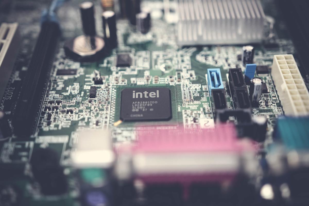
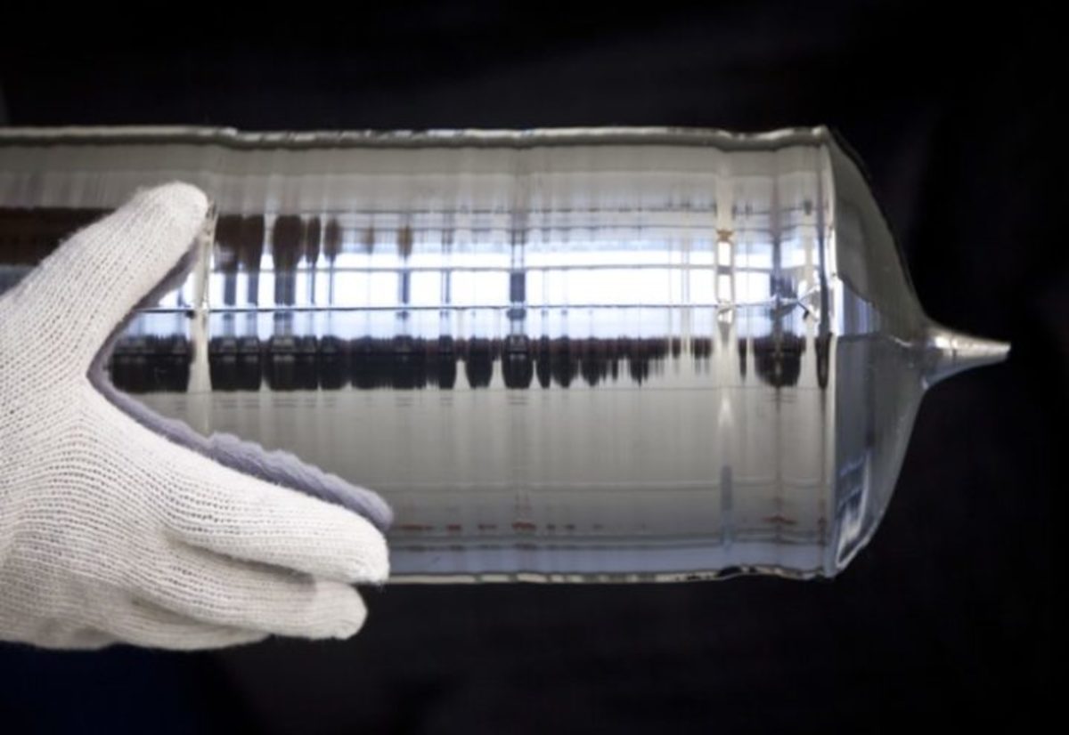
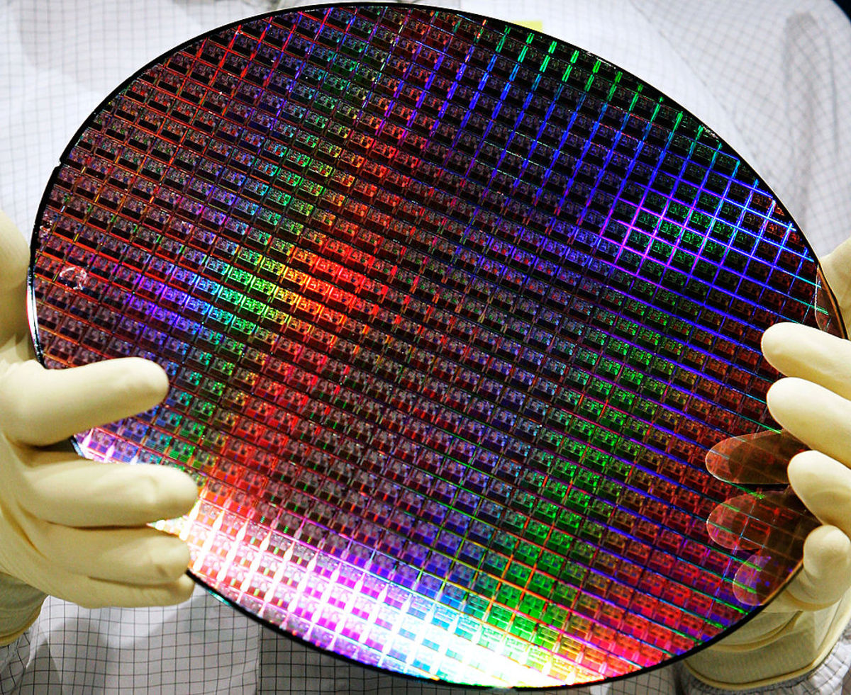
IEEE Spectrum These factories run 24 hours a day, only rarely closing for holidays or emergencies. It is most common to have 10 or 12 hour shifts that rotate between day and night employees. When inside of the cleanroom, workers must wear a full cleanroom suit, but this is not to protect them. Rather, it is to protect the wafers from being contaminated with hair, dust, dirt, and tiny particles from the worker. A small flake of dust can ruin a semiconductor chip just by falling on it, and that can mean a lot of money wasted. There are also special air conditioning systems that circulate the air to remove any particles that escape the workers’ suits. Pok Rie Usually at a separate factory, the silicon is first artificially grown into large cylinders, known as ingots. These cylinders are then cut into perfectly round, thin wafers which look like a mirror on both sides, and shipped to the cleanroom to be processed. They come in different sizes depending on the capabilities of the factory. The semiconductor cleanroom uses heavy chemicals and complex chemical processes to slowly build up precise layers onto the wafers. These layers are so thin that you would need a microscope to see them, and underneath one they look like an aerial view of a city. To the naked eye, a completed wafer looks iridescent with many different colors. Once the chemical layers and electrical charges are built up on the wafers, they are sent to yet another factory to have wires connected to them, making them a completed and functional semiconductor. Susoltech When these wafers are being made, there are many different types of machinery that the wafers travel through for each necessary chemical process. These are so complicated and involved that a wafer can take a year or more of constant chemical processing (and travelling between machines) before it is complete. A single wafer can cost upwards of $20,000 depending on its use, so you can see why the long production time frame is worth waiting for! iTech Post These machines have processes that require radioactivity, highly reactive chemical exposures, use of lasers, magnetic fields, and photolithography (a similar concept to developing film from a camera, but more complicated). They are operated by a combination of people and robots depending on how sophisticated a particular cleanroom is. Exhaust systems are connected to each machine and the wafers get processed inside of each sealed machine, but these are not always fool proof safety systems. There are so many heavy chemicals, man-made and natural, which would not be found in the every day world. This creates a high-risk environment for employees whenever something goes wrong since the special air filtration systems do not always remove gases from the air. To see a cleanroom in action, watch the music video below:
Such Great Heights by The Postal Service
My First Impression
When I first interviewed for a job in a semiconductor factory, my number one concern was, “Is this safe?” So I researched as much as I could online about the semiconductor processes that produce these electronic resistors. Other than general information about how the cleanroom operates as a whole, I was surprised to find very little information on the health risks. I found many sources which talked about the dangers of the industry in the 1990s, but current info was lacking. Why is that? I decided to take the job and see for myself. I was surprised to see all kinds of chemical labels on the machinery I would be spending 12 hours a day with. Tetraethylorthosilicate, hydrofluoric acid, fluorine, and arsenic were just a few. Those labels scared me! But the weird thing is that my coworkers, the people who had been working there 20+ years, thought nothing of it. I asked them about the labels and none of them seemed to have given it a second thought other than, “Yes they are dangerous, but we aren’t handling them directly so there’s nothing to worry about.” Okay, I guess. I worked in that first semiconductor cleanroom for 2 years, and never got sick. But I worked with tools that had “WARNING: Ionizing Radiation” symbols on them. I put my hands inside equipment that still had warm air inside from baking chemicals into the silicon wafers. Who knows what the long term effects are? Especially for people working there for over twenty years. I’ve read articles about people working in the Korean semiconductor industry who had miscarriages or birth defects because of the chemicals used in their department. Although I am in the US (which has higher safety standards), I worked in the same department those people did. They claimed to have gotten rid of those chemicals that cause reproductive issues in women, but how can I truly be sure that none of the other chemicals I was exposed to could cause the same issues?
The Health Risk
We want to believe everything in manufacturing is safe, but the truth is that the semiconductor industry is able to cover things up by calling it a “trade secret”. As a result, very few studies are implemented about the long term effects of chemical exposure on workers, and majority of the studies and safety checks are regulated internal to the company being reviewed. In my own personal experience, I used to spend 6 hours a day sitting above equipment called scrubbers, which use a slurry of chemicals to clean silicone wafers between processing steps. I have seen the chemical info on the equipment before (since they are legally required to list it), and it literally says “slurry” because there are so many different chemicals mixed together that they don’t list them all. There were holes in the floor below where I sat to account for air circulation, so whenever those scrubbers leaked, you can bet it went right up to where I was sitting. I have to wonder, how many chemicals am I breathing in? How often do those scrubbers leak? This article was written recently about the Korean semiconductor industry, and it’s really sad. Even now in the US, there are a lot of risks imposed by chemicals that are recirculated into the air of the deceptively named “cleanrooms”. Most people think of the industry as being all electronics, but it’s actually heavy chemicals that make all the chips for our phones, cars, etc. The US may be 25 years ahead of Korea in health safety but as long as heavy chemicals are being used, there will always be a higher exposure risk to anyone working inside the cleanroom.
The Future
Things have improved massively since the start of the industry, with more emphasis being placed on worker safety and hazard awareness. But things still happen, especially with unexpected events (during power outages, there is a huge risk of sitting chemicals, which means that toxic gases can form if left sitting for too long). As an ordinary person, I never expected to know what fluorine smells like, but unfortunately some things just come with the job. I will continue working in semiconductor, and my cautious thoughts that were born in my first interview will stick with me as long as I live. What do you think? Do you have any questions? Post below. This content is accurate and true to the best of the author’s knowledge and is not meant to substitute for formal and individualized advice from a qualified professional. © 2019 Rebecca Swafford
Comments
Liz Westwood from UK on January 01, 2020: This is an interesting article. It lifts the lid on an industry that I have little knowledge of. I think you are right to be wary of health risks. Too often developments in technology run ahead of safety checks.